

Diagram Of An Open Circuit
The phototransistor concept was known for the past many years. The first idea was proposed past William Shockley in the year 1951, later the discovery of a normal bipolar transistor. After two years, a phototransistor was demonstrated. After that, it was used in different applications, and mean solar day past day its evolution was continued. Phototransistors are extensively obtainable with low price from the distributors of electronic components to use in different electronic circuits. A semiconductor device like a phototransistor is used to detect the light levels and changes the flow of current among emitter & collector terminals based on the light level it gets. This article discusses an overview of phototransistors.
What is Phototransistor?
A Phototransistor is an electronic switching and electric current amplification component which relies on exposure to lite to operate. When light falls on the junction, reverse current flows which are proportional to the luminance. Phototransistors are used extensively to detect light pulses and convert them into digital electrical signals. These are operated past light rather than electric electric current. Providing a large amount of proceeds, low cost and these phototransistors might be used in numerous applications.
It is capable of converting light energy into electrical energy. Phototransistors work in a like way to photoresistors commonly known as LDR (low-cal dependent resistor) but are able to produce both current and voltage while photoresistors are only capable of producing electric current due to change in resistance.
Phototransistors are transistors with the base terminal exposed. Instead of sending current into the base, the photons from striking light activate the transistor. This is because a phototransistor is fabricated of a bipolar semiconductor and focuses on the free energy that is passed through it. These are activated past light particles and are used in near all electronic devices that depend on low-cal in some mode. All silicon photosensors (phototransistors) respond to the entire visible radiation range equally well every bit to infrared. In fact, all diodes, transistors, Darlington's, TRIACs, etc. have the same basic radiation frequency response.
The construction of the phototransistor is specifically optimized for photo applications. Compared to a normal transistor, a phototransistor has a larger base of operations and collector width and is made using diffusion or ion implantation.
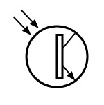
Structure
A phototransistor is nada simply an ordinary bi-polar transistor in which the base region is exposed to illumination. It is available in both the P-Northward-P and N-P-N types having different configurations like mutual emitter, common collector, and common base but generally, common emitter configuration is used. It tin as well work while the base of operations is made open up. Compared to the conventional transistor it has more base and collector areas.

Ancient phototransistors used single semiconductor materials like silicon and germanium simply at present a twenty-four hours's modern components use materials like gallium and arsenide for high-efficiency levels. The base is the atomic number 82 responsible for activating the transistor. It is the gate controller device for the larger electrical supply. The collector is the positive lead and the larger electric supply. The emitter is the negative lead and the outlet for the larger electrical supply.
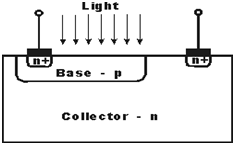
With no calorie-free falling on the device in that location will exist a pocket-sized current flow due to thermally generated hole-electron pairs and the output voltage from the excursion will be slightly less than the supply value due to the voltage driblet across the load resistor R. With light falling on the collector-base junction the current period increases. With the base connectedness open circuit, the collector-base of operations current must flow in the base of operations-emitter excursion, and hence the electric current flowing is amplified by normal transistor action.
The collector-base junction is very sensitive to low-cal. Its working condition depends upon the intensity of light. The base of operations current from the incident photons is amplified by the gain of the transistor, resulting in current gains that range from hundreds to several thou. A phototransistor is l to 100 times more sensitive than a photodiode with a lower level of noise.
How Does a Phototransistor Work?
A normal transistor includes an emitter, base, and collector terminals. The collector terminal is biased positively relating to the emitter terminal & the BE junction is reverse biased.
A phototransistor activates once the lite strikes the base terminal & the light triggers the phototransistor past allowing the configuration of hole-electron pairs likewise as the electric current menstruation across the emitter or collector. When the current increases, and then it is concentrated likewise as changed into voltage.
Generally, a phototransistor doesn't include a base connection. The base terminal is disconnected as the low-cal is used to allow the flow of current to supply throughout the phototransistor.
Types of Phototransistor
Phototransistors are classified into two types namely BJT and FET.
BJT Phototransistor
In the deficiency of light, BJT phototransistor allows leakage among collectors as well as an emitter of 100 nA otherwise low. Once this transistor is exposed to the beam, information technology performs upto 50mA. This distinguishes information technology from photodiode which cannot let much electric current.
FET Phototransistor
This kind of phototransistor includes two terminals that connect within through its collector & emitter otherwise source & drain within FET. The transistor'due south base last reacts to light & controls the electric current menstruum among the terminals.
Phototransistor Circuit
A phototransistor works only like a normal transistor, where the base electric current is multiplied to give the collector electric current, except that in a phototransistor, the base electric current is controlled by the amount of visible or infrared low-cal where the device only needs 2 pins.
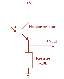
In the simple circuit, assuming that nothing is connected to Vout, the base of operations current controlled by the amount of light will make up one's mind the collector electric current, which is the current going through the resistor. Therefore, the voltage at Vout volition motion high and low based on the amount of low-cal. We tin can connect this to an op-amp to heave the signal or directly to an input of a microcontroller.
The output of a phototransistor is dependent upon the wavelength of the incident light. These devices reply to light over a broad range of wavelengths from the near UV, through the visible, and into the near IR part of the spectrum. For a given light source illumination level, the output of a phototransistor is defined past the surface area of the exposed collector-base junction and the dc electric current gain of the transistor
Phototransistors are bachelor in different configurations like optoisolator, optical switch, retro sensor. Optoisolator is similar to a transformer in that the output is electrically isolated from the input. An object is detected when it enters the gap of the optical switch and blocks the low-cal path between the emitter and detector. The retro sensor detects the presence of an object by generating light and so looking for its reflectance off of the object to be sensed.
Amplification
The operation range of a phototransistor mainly depends on the practical light intensity because its operating range is dependent on the input of the base. The current of the base concluding from the incident photons tin can exist amplified through the transistor's proceeds, which results in a current gain that ranges from 100 to 1000. A phototransistor is more sensitive equally compared to a photodiode through a less dissonance level.
Actress amplification can be supplied through a photodarlington-type transistor.
This is a phototransistor including an emitter output that is connected to the base of operations terminal of the next bipolar transistor. It gives loftier sensitivity within the levels of low low-cal as it provides a current gain that is equivalent to the two transistors. The proceeds of the two stages tin offer net gains college than 100,000A. A photodarlington transistor includes less response as compared to a normal phototransistor.
Modes of Operation
In phototransistor circuits, the basic modes of operation include two similar active & switch where the commonly used mode of operation is switch blazon. Information technology explains a not-linear response toward the light; one time there is no low-cal and then at that place is no flow of current into the transistor. Electric current starts to supply similar exposure toward light increases. The switch-mode works in an ON/OFF system. Active fashion is also called a linear that reacts in such a manner that, it is proportional toward the low-cal stimulus.
Performance Specifications
The selection of Phototransistor tin exist done depending on different parameters as well as specifications similar the following.
- Collector Current (IC)
- Base Electric current (Iλ)
- Acme Wavelength
- Collector-to-Emitter Breakdown Voltage (VCE)
- Collect-emitter breakup voltage (VBRCEO)
- Emitter-collector breakdown voltage (VBRECO)
- Night current (ID)
- Ability dissipation (PD or Ptot)
- Ascent time (tR)
- Fall time (tF)
Design Parameters
The selected materials, as well equally composition, play an essential office in the sensitivity of this type of transistor. The gain level of Homo-structure or unmarried material devices ranges from 50 to several hundred. These are normal phototransistors that are frequently designed with silicon. The heterostructure devices or several material configuration devices may include gain levels upwards to 10k but they are less common dues to high production costs.
- The electromagnetic wavelength range of different materials include the post-obit,
- For Silicon (Si) material, the electromagnetic wavelength range is 190 to 1100 nm
- For Germanium (Ge) material, the electromagnetic wavelength range is 400 to 1700 nm
- For Indium gallium arsenide (InGaAs) fabric, the electromagnetic wavelength range is 800 to 2600 nm
- For Atomic number 82 sulfide material, the electromagnetic wavelength range is <thousand to 3500
- For the proper function of a phototransistor, mounting technology plays a key role.
The SMT or surface mount applied science uses components to a PCB (printed circuit board) by connecting the component terminals through soldering otherwise to the top face of the board. Ordinarily, the printed excursion board pad can be coated using a paste such every bit a solder & flux conception. High temperatures unremarkably from an infrared oven will dissolve the paste to solder the terminals of component toward the PCB pads.
THT or through-hole engineering science is a commonly utilized mounting style. The arrangement of components tin can be washed by placing component terminals using holes inside the PCB & these components can be soldered in the contrary face of the PCB. The features of phototransistors mainly include a cutoff filter, used to cake observable light. The light detection in others can exist improved through an anti-cogitating coating. Devices including a round dome lens in place of a flat lens are also obtainable.
Photodiode Vs Phototransistor
The departure between photodiode and phototransistor includes the post-obit.
| Photodiode | Phototransistor |
| The photodiode is a PN-junction diode, used to generate electric current in one case a photon of light strikes on their surface. | The phototransistor is used to change the free energy of the calorie-free into an electrical energy |
| It is less sensitive | It is more than sensitive |
| The output response of photodiode is fast | The output response of the phototransistor is low |
| It produces current | It produces voltage and current |
| Information technology is used in solar power generation, detecting UV otherwise IR rays & also for low-cal measuring, etc. | Information technology is used in compact disc players, smoke detectors, lasers, invisible light receivers, etc. |
| It is more reactive to incident lights | Information technology is less reactive |
| The photodiode has a less dark electric current | Phototransistor has loftier nighttime current |
| In this, both the biasing is used like frontwards and reverse | In this, forrard biasing is used |
| The linear response range of photodiode is much wider | The linear response range of phototransistor is much lower |
| Photodiode allows low current as compared to a phototransistor | Phototransistor allows high current every bit compared to the photodiode |
| The photodiode is used for bombardment-powered devices that apply less power. | The phototransistor is used as a solid-state switch, non like a photodiode. |
Characteristics
The characteristics of a phototransistor include the post-obit.
- Low-cost visible and about-IR photodetection.
- Bachelor with gains from 100 to over 1500.
- Moderately fast response times.
- Available in a broad range of packages including epoxy-coated, transfer-molded, and surface mounting technology.
- Electrical characteristics were similar to that of signal transistors.
Advantages of Phototransistor
Phototransistors have several important advantages that split them from another optical sensor some of them are mentioned beneath
- Phototransistors produce a college current than photodiodes.
- Phototransistors are relatively cheap, simple, and minor plenty to fit several of them onto a single integrated calculator bit.
- Phototransistors are very fast and are capable of providing nearly instantaneous output.
- Phototransistors produce a voltage, that photo-resistors cannot do then.
Disadvantages of Phototransistor
- Phototransistors that are made of silicon are non capable of handling voltages over 1,000 Volts.
- Phototransistors are likewise more vulnerable to surges and spikes of electricity likewise as electromagnetic free energy.
- Phototransistors as well do not permit electrons to movement as freely as other devices do, such as electron tubes.
Applications of Phototransistors
The Areas of application for the Phototransistor include:
- Punch-card readers.
- Security systems
- Encoders – measure speed and direction
- IR detectors photo
- electric controls
- Calculator logic circuitry.
- Relays
- Lighting control (highways etc)
- Level indication
- Counting systems
Thus, this is all about an overview of a phototransistor. From the higher up data finally, we tin conclude that phototransistors are widely used in different electronic devices for detecting light such every bit infrared receivers, fume detectors, lasers, CD players, etc. Here is a question for you, what is the difference between phototransistor and photodetector?

Diagram Of An Open Circuit,
Source: https://www.elprocus.com/phototransistor-basics-circuit-diagram-advantages-applications/
Posted by: campbelltrailtoo.blogspot.com

0 Response to "Diagram Of An Open Circuit"
Post a Comment